Product description
The AD636 is a low power monolithic IC that performs true RMS-to-DC conversion on low level signals. It offers performance that is comparable or superior to that of hybrid and modular converters costing much more. The AD636 is specified for a signal range of 0 mV to 200 mV rms. Crest factors up to 6 can be accommodated with less than 0.5% additional error, allowing accurate measurement of complex input waveforms. The low power supply current requirement of the AD636, typically 800 µA, is ideal for battery-powered portable instruments. It operates from a wide range of dual and single power supplies, from ±2.5 V to ±16.5 V or from +5 V to +24 V. The input and output terminals are fully protected; the input signal can exceed the power supply with no damage to the device (allowing the presence of input signals in the absence of supply voltage), and the output buffer amplifier is short-circuit protected. The AD636 includes an auxiliary dB output derived from an internal circuit point that represents the logarithm of the rms output. The 0 dB reference level is set by an externally supplied current and can be selected to correspond to any input level from 0 dBm (774.6 mV) to -20 dBm (77.46 mV). Frequency response ranges from 1.2 MHz at 0 dBm to greater than 10 kHz at -50 dBm. The AD636 is easy to use. The device is factory-trimmed at the wafer level for input and output offset, positive and negative waveform symmetry (dc reversal error), and full-scale accuracy at 200 mV rms. Therefore, no external trims are required to achieve full-rated accuracy.
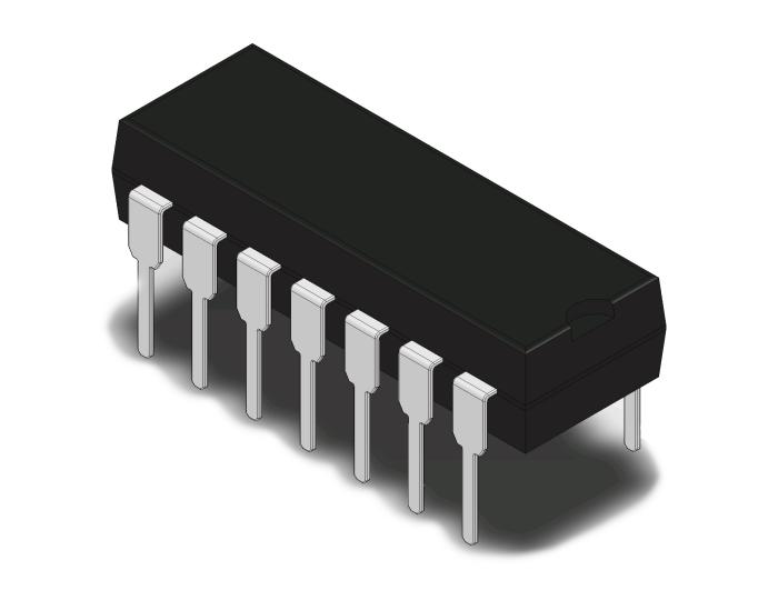
The AD636 is available in two accuracy grades. The total error of the J-version is typically less than ±0.5 mV ± 1.0% of reading, while the total error of the AD636K is less than ±0.2 mV to ±0.5% of reading. Both versions are temperature rated for operation between 0°C and 70°C and available in 14-lead SBDIP and 10-lead TO-100 metal can. The AD636 computes the true root-mean-square of a complex ac (or ac plus dc) input signal and gives an equivalent dc output level. The true rms value of a waveform is a more useful quantity than the average rectified value because it is a measure of the power in the signal. The rms value of an ac-coupled signal is also its standard deviation. The 200 mV full-scale range of the AD636 is compatible with many popular display-oriented ADCs. The low power supply current requirement permits use in battery-powered hand-held instruments. An averaging capacitor is the only external component required to perform measurements to the fully specified accuracy is. Its value optimizes the trade-off between low frequency accuracy, ripple, and settling time. An optional on-chip amplifier acts as a buffer for the input or the output signals. Used in the input, it provides accurate performance from standard 10 MO input attenuators. As an output buffer, it sources up to 5 mA.
* True rms-to-dc conversion * 200 mV full scale * Laser-trimmed to high accuracy (1.0% maximum error)
* Wide response capability * Computes rms of ac and dc signals * 1 MHz, -3 dB bandwidth: V rms > 100 mV * Signal crest factor of 6 for 0.5% error * dB output with 50 dB range * Low power: 800 µA quiescent current * Single or dual supply operation

