


Product description
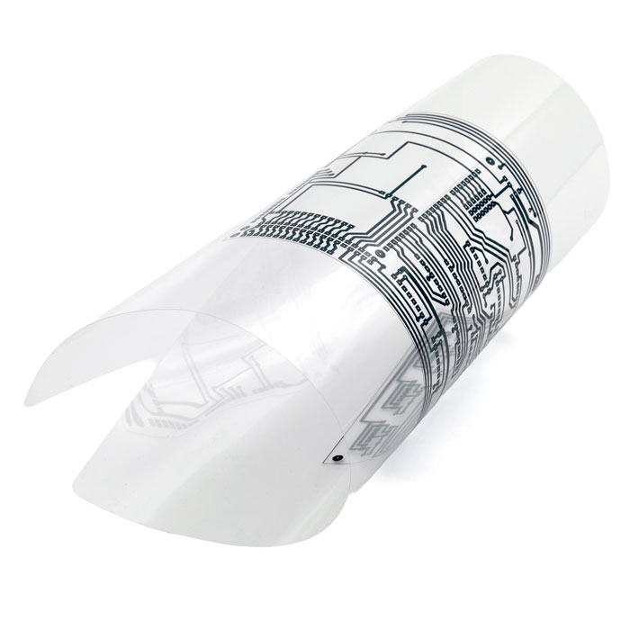
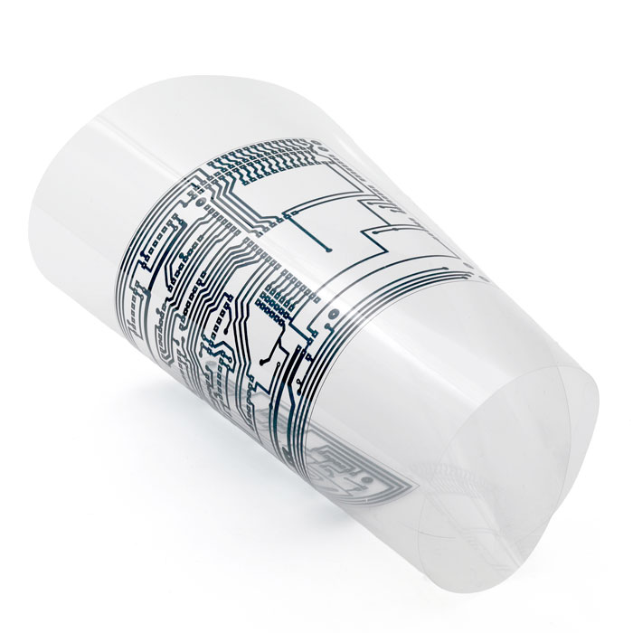
Transparent A4 film for use with photoresist-coated PCBs. The film is designed for inkjet printers and is used to transfer circuit patterns onto UV-sensitive photoresist.
The PCB layout is printed onto the film using a inkjet printer. The black areas block UV light, while the transparent areas allow UV light to pass through to the photoresist. This allows conductive traces and other details to be transferred to the PCB with high precision.
Instructions for use:
-
Print the PCB layout onto the film using an inkjet printer. Use the highest possible print quality and black ink density. The film has two sides, one of which has a slightly matte surface. Print on the matte side.
-
Place the film directly against the photoresist layer on the PCB. Make sure the film lies flat and flush against the photoresist surface. A glass plate can be used to ensure good contact between the film and the photoresist.
-
Expose the PCB to UV light through the film. Experiment to determine the appropriate exposure time and distance. The exposure time depends on the intensity of the UV light source, the wavelength of the UV light (ideally 365 nm) and the distance to the PCB.
-
Develop the PCB using a developer suitable for photoresist. Follow the manufacturer's instructions for the correct mixing ratio of developer powder to water.
-
After development, the PCB can be etched to create the desired conductive trace pattern.